555 Timer: Internal Operation and Monostable Mode
The 555 timer is a timing IC that turns a few external resistors and capacitors into delays, pulses, oscillators, alarms, LED flashers, and simple control circuits. This lesson focuses on the internal operation and monostable, or one-shot, mode.
Learning Objectives
By the end of this lesson, you should be able to identify the 555 pins, explain the 1/3 Vcc and 2/3 Vcc thresholds, calculate monostable pulse width, choose practical timing parts, and debug common one-shot failures.
What the 555 Contains
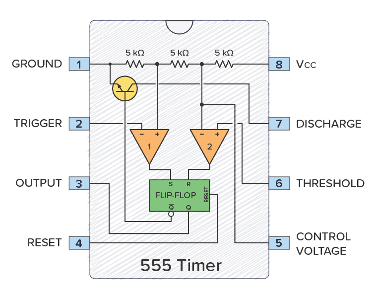
Inside a bipolar 555 are:
- a three-resistor divider that creates
1/3 Vccand2/3 Vcc; - two comparators;
- an SR latch;
- a discharge transistor connected to pin 7;
- an output driver on pin 3;
- a reset input on pin 4;
- a control-voltage input on pin 5.
The divider is why the 555 switches at predictable fractions of the supply voltage.
Pin Functions
- Pin 1,
GND: circuit return. - Pin 2,
TRIG: when below1/3 Vcc, sets the latch and drives output high. - Pin 3,
OUT: timing output. - Pin 4,
RESET: active low; tie high for normal operation. - Pin 5,
CTRL: adjusts comparator thresholds; usually bypass with10 nF. - Pin 6,
THRES: when above2/3 Vcc, resets the latch and drives output low. - Pin 7,
DISCH: open-collector/open-drain style discharge switch to ground. - Pin 8,
Vcc: positive supply.
For a 5 V supply:
$$
V_{TRIG} = \frac{1}{3}V_{cc} = 1.67 V
$$
$$
V_{THRES} = \frac{2}{3}V_{cc} = 3.33 V
$$
Monostable Mode
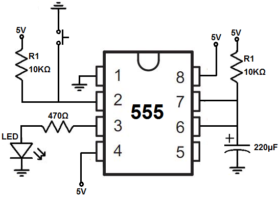
In monostable mode, the 555 produces one timed output pulse after a trigger.
Typical connections:
- pin 8 and pin 4 to
Vcc; - pin 1 to ground;
- pin 5 to ground through
10 nF; - pin 2 pulled high and momentarily driven low by the trigger;
- timing resistor from
Vccto pins 6 and 7; - timing capacitor from pins 6 and 7 to ground;
- output on pin 3.
Timing Formula
When triggered, the discharge transistor turns off and the capacitor charges through R. The pulse ends when the capacitor reaches 2/3 Vcc.
$$
T = 1.1RC
$$
where T is seconds, R is ohms, and C is farads.
Try It: 555 Monostable Calculator
Enter any two values and leave the third empty.
Formula: `T = 1.1 R C`.
Worked Example: 10 Second Delay
Goal: output high for about 10 s after a button press.
Choose C = 100 uF.
$$
R = \frac{T}{1.1C}
= \frac{10}{1.1 \times 100 \times 10^{-6}}
= 90.9 k\Omega
$$
Use 91 kOhm. Use a low-leakage capacitor if timing accuracy matters; electrolytic leakage can noticeably shorten or lengthen long delays.
Step-by-Step Operation
- Idle: output is low and pin 7 discharges the timing capacitor.
- Trigger: pin 2 goes below
1/3 Vcc, setting the latch. - Timing: output goes high, pin 7 opens, and the capacitor charges through
R. - Threshold: pin 6 reaches
2/3 Vcc, resetting the latch. - Reset: output goes low and pin 7 discharges the capacitor.
The trigger pulse should return high before the timing interval ends. If pin 2 is held low, the output can remain high or retrigger unexpectedly.
Choosing Timing Components
- Keep timing resistance above about
1 kOhmto limit discharge current. - Avoid very high resistance above about
1 Mohmto10 Mohmunless leakage is controlled. - Use C0G/film capacitors for short accurate times.
- Use low-leakage electrolytics or tantalum only when long timing intervals require large capacitance.
- For minutes or hours, use a counter, RTC, or microcontroller instead of a simple RC 555 timer.
Applications
- Button debouncing with a
10 msto50 mspulse. - Pulse stretching so a short sensor event is visible to logic.
- Power-on reset or startup delay.
- Missing-pulse detection when a periodic signal stops.
- Simple timeouts and alarms.
Practical Build Checks
- Tie reset pin 4 high; never leave it floating.
- Add
10 nFfrom control pin 5 to ground. - Decouple pin 8 to pin 1 with
100 nFclose to the IC. - Confirm trigger voltage falls below
1/3 Vcc. - Confirm threshold capacitor voltage rises to
2/3 Vcc. - Check output load current against the selected 555 variant.
Common Mistakes
- Floating trigger input causing random pulses.
- Floating reset input holding the output low.
- Reversing an electrolytic timing capacitor.
- Choosing
Rso low that pin 7 current is excessive. - Expecting precision timing from high-leakage capacitors.
- Forgetting that bipolar and CMOS 555 variants have different output drive and supply-current behavior.
Summary
The 555 monostable is a hardware one-shot. A low pulse on pin 2 starts the output pulse, the timing capacitor charges, and pin 6 ends the pulse at 2/3 Vcc. The core formula is T = 1.1RC, but reliable circuits also need pull-ups, reset wiring, control-pin bypassing, supply decoupling, and realistic timing components.
Further Reading
- Texas Instruments, NE555 and TLC555 datasheets.
- Analog Devices, "TimerBlox and Timer Circuit Design Notes."
- Horowitz and Hill, The Art of Electronics, timing circuits.
- Manufacturer application notes for monostable and watchdog 555 circuits.